
0
Owner's of the Agilent Technologies Video Gaming Accessories Agilent Technologies Video Gaming Accessories gave it a score of 0 out of 5. Here's how the scores stacked up:

Chapter 4 Theory of Operation
Floating Logic
82
Floating Logic
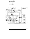
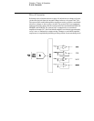
Referring to the schematic shown on page 124, the floating common logic
controls operation of the entire instrument. All output functions and bus
command interpretation is performed in the main controller U17. The front
panel and the earth referenced logic operate as slaves to U17. The floating
common logic is comprised of the main controller U17, custom gate array U16,
the program ROM U13, RAM U14, calibration EEPROM U15, and the 12 MHz
clock oscillator. Non-volatile EEPROM U15 stores calibration constants,
calibration secure code, and calibration count, and store/recall variables.
Power-on reset is provided to the main controller by the voltage regulator U11.
The main controller U17 is a 16-bit micro controller. It controls such features
as receive and transmit serial port, timer/counter ports, an 8-bit pulse width
modulated DAC port, and selectable input 10-bit successive approximation a-
to-d convert ports. A conventional address/data bus is used to transfer data
between the main controller and external ROM and RAM. When the address
latch enable (ALE) signal goes high, address data is present on the address/
data bus. ASIC U18 latches the address data and decodes the correct chip
enable (low true) for external ROM and RAM accesses and for read/write
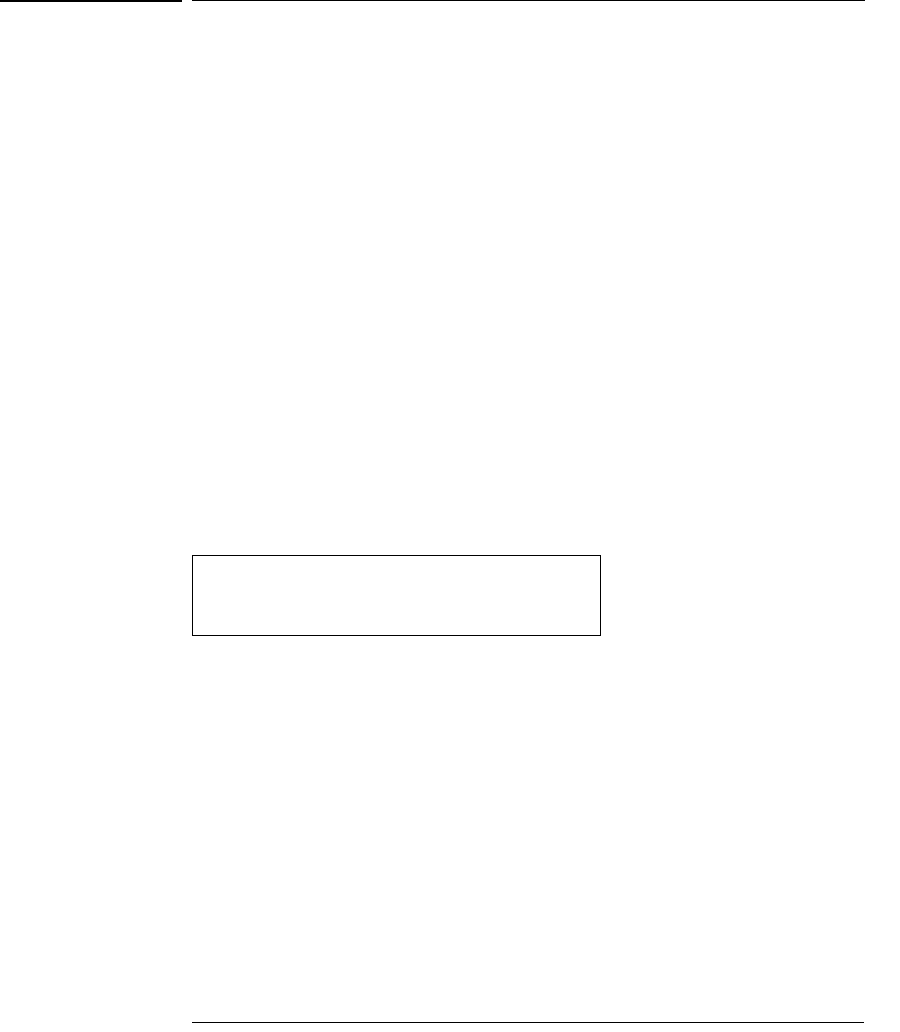
accesses to the internal registers of U18. The system memory map is shown
below.
Program ROM U13 contains four 64k x 8 data banks of data. Banks are selected
by controlling A16 and A17 ROM address bits directly from the main controller
port bits.
Custom gate array U18 performs address latching and memory map decoding
functions as discussed above. In addition, U18 contains a variety of internal
read/write registers. The read (XRD) and write (XWR) signals transfer data out
of and into U18 when it is addressed. There are four internal registers in U18:
an internal configuration register, an 8 bit counter register, a serial transmit/
receive register, and an internal status register.
The counter register is used to capture the ADC slope count at the COMP input.
The COMP input functions as both a clocked comparator and the slope counter
input for the ADC. In both cases the counter register captures the lower 8 bits
of a 24-bit counter. The upper 16 bits of the count are captured by the SYNC
input to U17.
0000
H
- 1FF7
H
U15 32k x 8 RAM
1FF8
H
- 1FFF
H
U16 Gate Array
2000
H
- FFFF
H
U14 Program ROM


Find Your Products By Category
- Household Appliance
- Power Tools
- Computer Equipment
- Automotive
- TV and Video
- Outdoor Cooking
- Marine Equipment
- Kitchen Appliance
- Fitness & Sports
- Lawn and Garden
- Baby
- Laundry Appliance
- Personal Care
- Home Audio
- Photography
- Video Game
- Portable Media
- Musical Instruments & Equipment
- Communications
- Car Audio and Video
Please Login
