

0
Owner's of the Agilent Technologies Welding System Agilent Technologies Welding System gave it a score of 0 out of 5. Here's how the scores stacked up:


Chapter 4 Theory of Operation
A-to-D Converter
87
4
A-to-D Converter
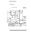
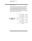
Referring to the schematic shown on page 129, the analog-to-digital converter
(ADC) is used to change dc voltages into digital information. The circuitry
consists of an integrator amplifier (U6 and U8), current steering switch U5,
resistors (R5, R4, R15 and R16), voltage reference (U3A and U3B), ADC
controller U16, and residue ADC U17 on the top board.
The ADC method used by the Agilent E3631A is called multislope III.
Multislope III is a charge balancing continuously integrating analog-to-digital
converter. The input voltage continuously forces charge onto the integrator
capacitors C18 and C19 through R15 on the top board.
Switch U5 steers fixed positive or negative reference currents onto the
integrator capacitors to cancel, or balance the accumulated input charge. The
level shifted (R19 and R20 on the top board) output of the integrator is checked
every 2.66
m
A by the U16 COMP input. Logic state machines in U16 control the
U5 current steering to continuously seek an approximate 2.5 V level on the
integrator amplifier output, FLASH. If the ADC input voltage ADC REF is
between ±15 V, the integrator output (FLASH) will remain within the 0 V to 5
V range of the U17 on-chip ADC. An input greater than +15 V may cause the
integrator output in U8 at pin 6 (U8-6) to saturate at about -15 V. An input less
than -15 V may cause U8 to saturate with an output of about +15 V. The U17
ADC input (FLASH) is clamped to 0 V or 5 V by R21 and CR3 to protect U17.
The integrator amplifier is formed by U6 and U8. Resistors R10 and R11 affect
the amplifier stability. Amplifier oscillation may occur if their values are
incorrect. Amplifier U6 improves the offset voltage characteristics of
integrator amplifier U8 on the top board.
Each analog-to-digital conversion occurs continuously. The ADC starts by
clearing the integrator slope count in U16. At the end of the integration period,
the slope count is latched. The slope count provides the most significant bits
of the input voltage conversion. The least significant bits are converted by the
on-chip ADC of U17.


Find Your Products By Category
- Household Appliance
- Power Tools
- Computer Equipment
- Automotive
- TV and Video
- Outdoor Cooking
- Marine Equipment
- Kitchen Appliance
- Fitness & Sports
- Lawn and Garden
- Baby
- Laundry Appliance
- Personal Care
- Home Audio
- Photography
- Video Game
- Portable Media
- Musical Instruments & Equipment
- Communications
- Car Audio and Video
Please Login
